
r-GeO₂ power semiconductorswill solve the world's energy problems.
r-GeO₂ power semiconductorswill solve the world's energy problems.
01
02
News
ServicesOur primary business involves the research, development, manufacturing, and sales of epitaxial wafers (substrates) for the new next-generation power semiconductor r-GeO₂ (rutile-type germanium dioxide).
Features of r-GeO2
High voltage, low energy loss
The high breakdown electric field ensures stable operation even in high-voltage environments, significantly reducing energy loss during power conversion. This contributes to higher system efficiency and heat
suppression.
Compact and lightweight
Low-loss characteristics enable device miniaturization, directly contributing to space-saving and weight reduction in end products. This enhances design flexibility and fosters the creation of new applications.
Environmentally friendly manufacturing process
The GeO₂ manufacturing process differs from the sublimation method for SiC (over 2000℃), as it enables production at film deposition temperatures below 1000℃. It also eliminates the need for expensive vacuum environments, significantly reducing power consumption, making it environmentally friendly, and
contributing to lower manufacturing costs. Furthermore, it is not as hard as SiC and lacks the cleavage
properties like gallium oxide, making device fabrication easier. This significantly contributes to improved device manufacturing yield and cost reduction.
High-quality crystals
Bulk crystals can be fabricated, and high-quality crystal films can be expected through homoepitaxial growth.
Contributing to an Energy-Saving Society
Reducing energy losses during power conversion contributes to lowering CO₂ emissions and helps realize a sustainable low-carbon society.
Unlocking new application
This enables high-power, high-voltage power control that was difficult with conventional semiconductors,driving new technological innovations across various fields such as industry and transportation
Basic Physical Properties Table for r-GeO₂
| Characteristics | r-GeO₂ |
|---|---|
| Bandgap (eV) | 4.45~4.77(Measured) |
| Breakdown field (MV/cm) | |
| Electron mobility (cm²/Vs)) | |
| Hole mobility (cm²/Vs) | |
| Thermal conductivity (W/m K) | |
| Average thermal expansion coefficient (/K) (Room temp. -600℃)((001) plane) | 3.9×10⁻⁶(Measured)* |
| Baliga’s Figure of Merit (Si=1) | |
| Vickers hardness (Hv) ((110) plane) | 1610 (Measured)* |
| Young’s modulus (GPa) | 293GPa(Measured)* |
The measured Bandgap (eV) values for r-GeO₂ (Rutile-type Germanium Dioxide) were published on September 7, 25.
(4.45-4.77 Patentix)
(The Bandgap value is 4.85-5.63 from literature).
*n=1.
The physical property values left blank are currently being measured. We will update them as soon as they are available for disclosure.
GeO2 Semiconductor Products
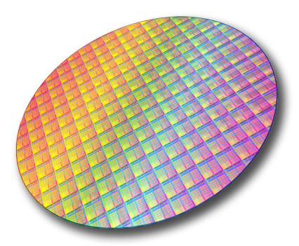
(開発中)
6inch substrate
(Under development)
Paid sample
10mm square
GeO₂ on TiO₂ substrate
(Paid samples available)
Product Photography
(Reference Photos)
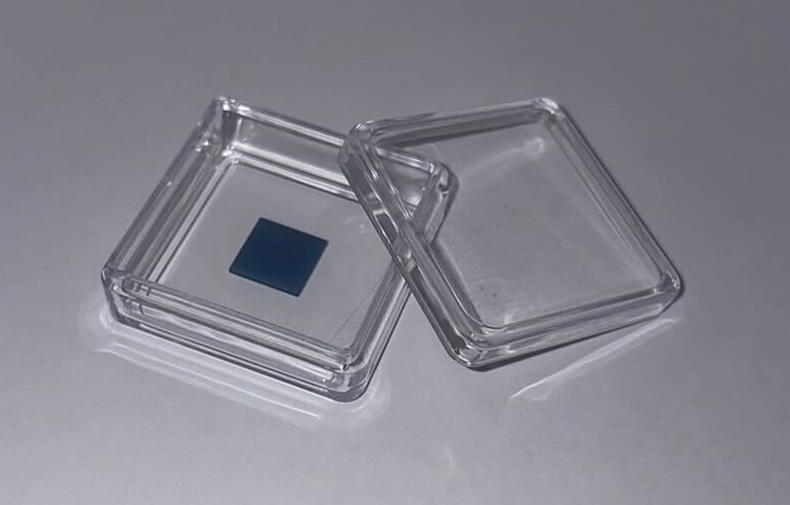
Specifications
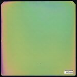
- Features: Rutile-type germanium dioxide films heteroepitaxially grown on a TiO₂ substrate with the same crystal structure as germanium dioxide.
- Doping: n-type doping with Antimony (Sb) is available.
- Substrate Size : 10mm square
For more details, please contact us.